Artículo
Halogen etching of Si via atomic-scale processes
Fecha de publicación:
26/09/2001
Editorial:
Elsevier
Revista:
Progress in Surface Science
ISSN:
0079-6816
Idioma:
Inglés
Tipo de recurso:
Artículo publicado
Clasificación temática:
Resumen
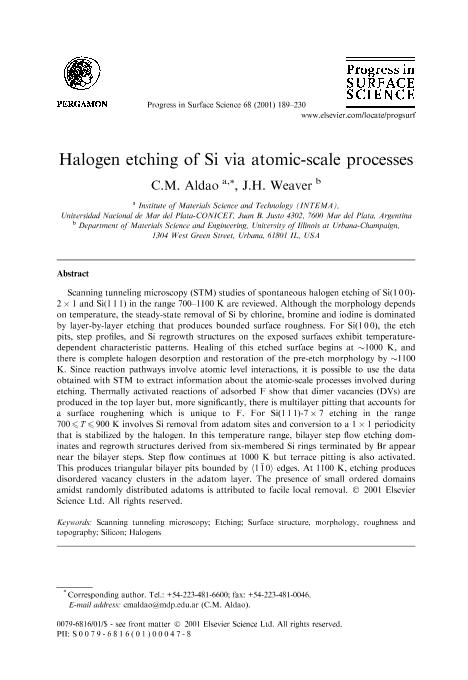
Scanning tunneling microscopy studies of spontaneous halogen etching of Si(100)-2x1 and Si(111) in the range 700–1100 K are reviewed. Although the morphology depends on temperature, the steady-state removal of Si by chlorine, bromine and iodine is dominated by layer-by-layer etching that produces bounded surface roughness. For Si(100), the etch pits, step profiles, and Si regrowth structures on the exposed surfaces exhibit temperature dependent characteristic patterns. Healing of this etched surface begins at ~1000 K, and there is complete halogen desorption and restoration of the pre-etch morphology by ~1100 K. Since reaction pathways involve atomic level interactions, it is possible to use the data obtained with STM to extract information about the atomic-scale processes involved during etching. Thermally-activated reactions of adsorbed F show that dimer vacancies are produced in the top layer but, more significantly, there is multilayer pitting that accounts for a surface roughening which is unique to F. For Si(111)-7x7 etching in the range 700 ≤ T ≤ 900 K involves Si removal from adatom sites and conversion to a 1x1 periodicity that is stabilized by the halogen. In this temperature range, bilayer step flow etching dominates and regrowth structures derived from six-membered Si rings terminated by Br appear near the bilayer steps. Step flow continues at 1000 K but terrace pitting is also activated. This produces triangular bilayer pits bounded by <1 0> edges. At 1100 K, etching produces disordered vacancy clusters in the adatom layer. The presence of small ordered domains amidst randomly distributed adatoms is attributed to facile local removal.
Archivos asociados
Licencia
Identificadores
Colecciones
Articulos(INTEMA)
Articulos de INST.DE INV.EN CIENCIA Y TECNOL.MATERIALES (I)
Articulos de INST.DE INV.EN CIENCIA Y TECNOL.MATERIALES (I)
Citación
Aldao, Celso Manuel; Weaver, J. H.; Halogen etching of Si via atomic-scale processes; Elsevier; Progress in Surface Science; 68; 4-6; 26-9-2001; 189-230
Compartir


